
thallia
Mock up PCB : binary watch
I soldered deep into the night….and all throughout today. After hours of writing and testing code, fiddling with hardware, and scraping through error after error, I can present to you the first mock up through-hole PCB!
I designed the schematic on EasyEDA:

And followed the setup from there. I’ll redo the schematic on EagleCAD because I was using EasyEDA mainly for the learning experience of using a different software. I could stand to make it a bit easier to look at, too.
Getting all my tools and supplies out, I pumped this guy out after a few hours:
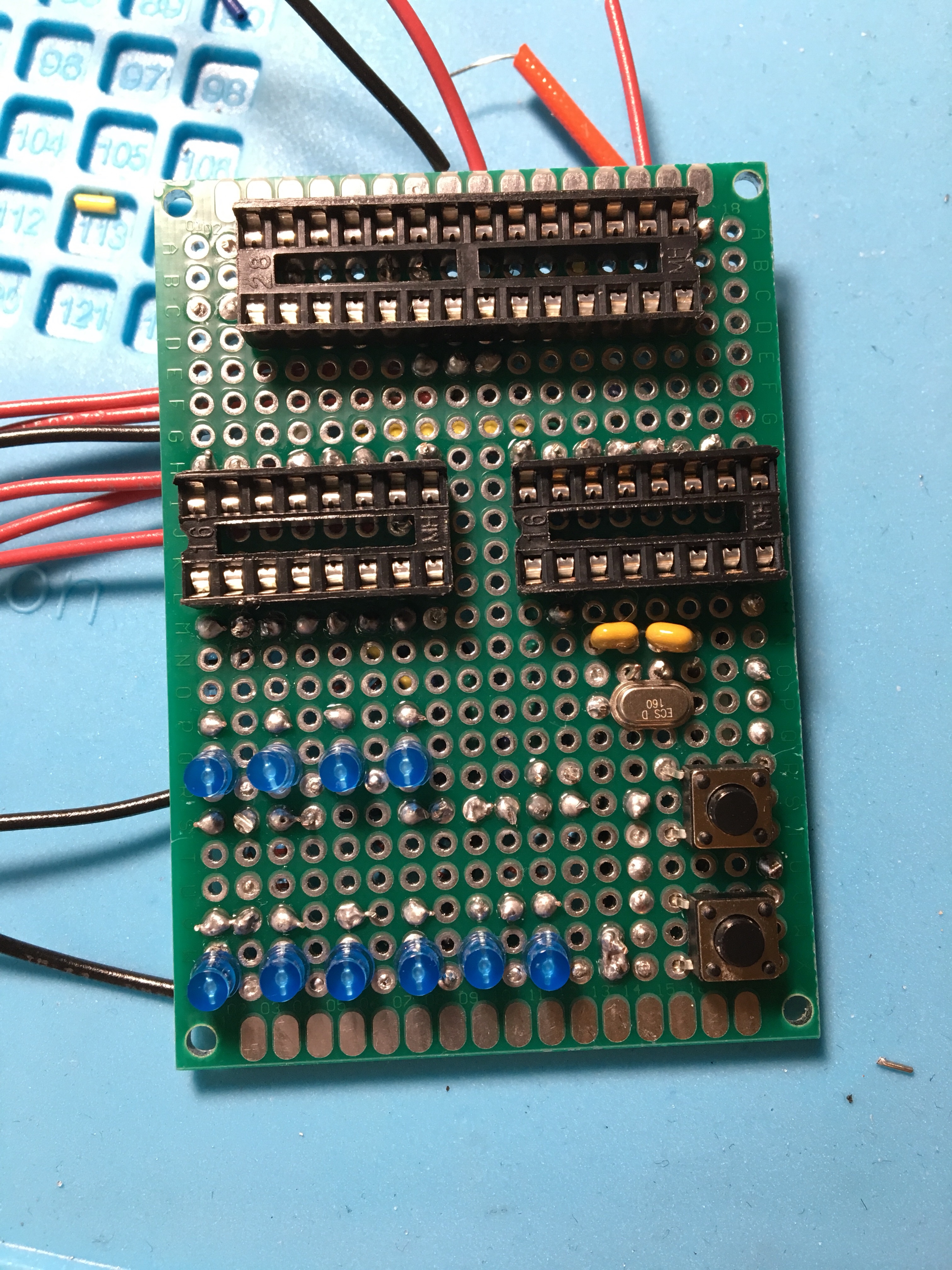

The connections on the back are a little gross, but I was excited to get it done! As you can see, I hadn’t had room to stick a coin cell battery holder, let alone the battery itself on the back, so made a smaller PCB that acted as the power source.This was slightly tricky, as I had to figure out what was GND and what was the power, and where I was supposed to connect all the wires to.
Top:
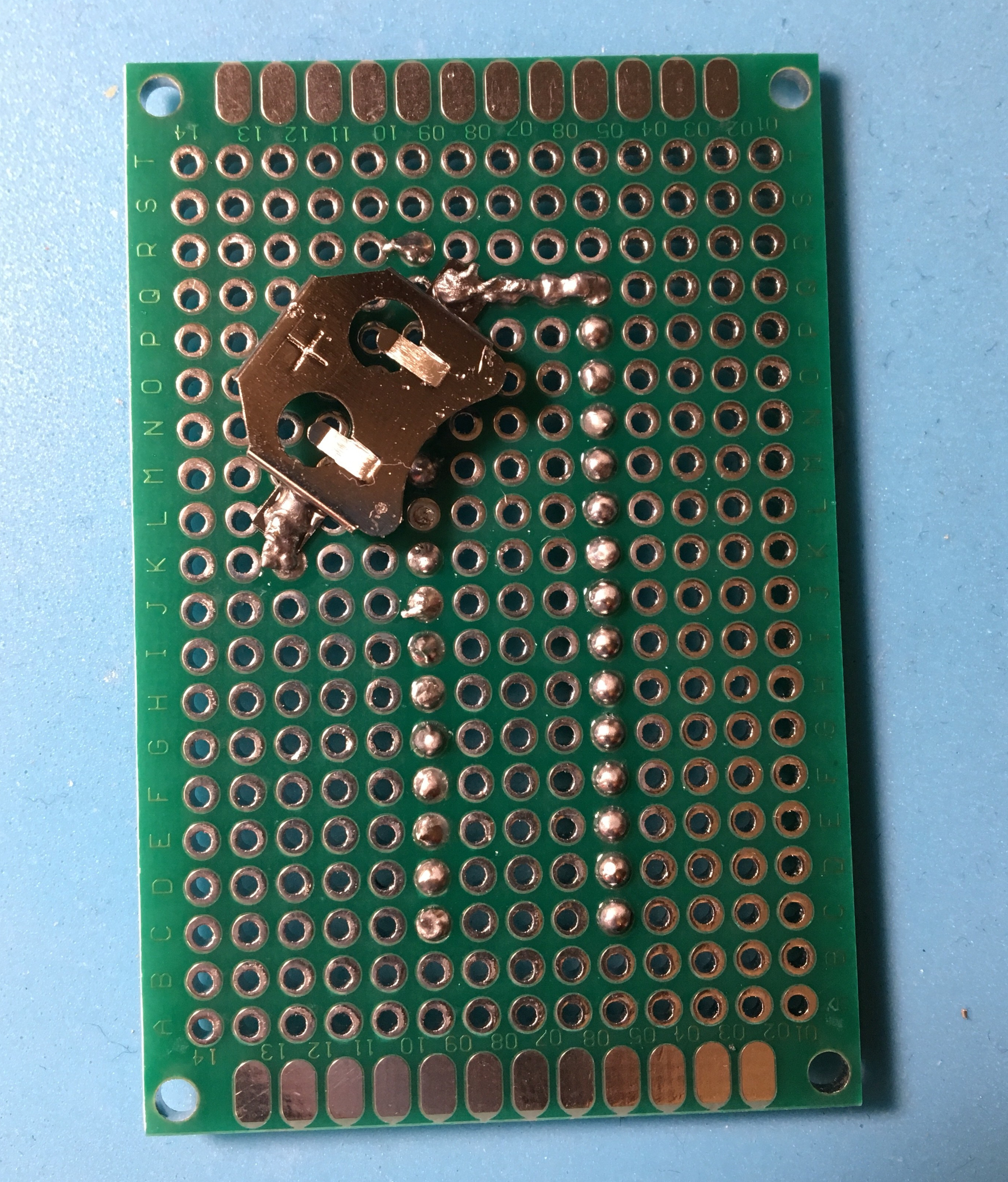
Bottom:

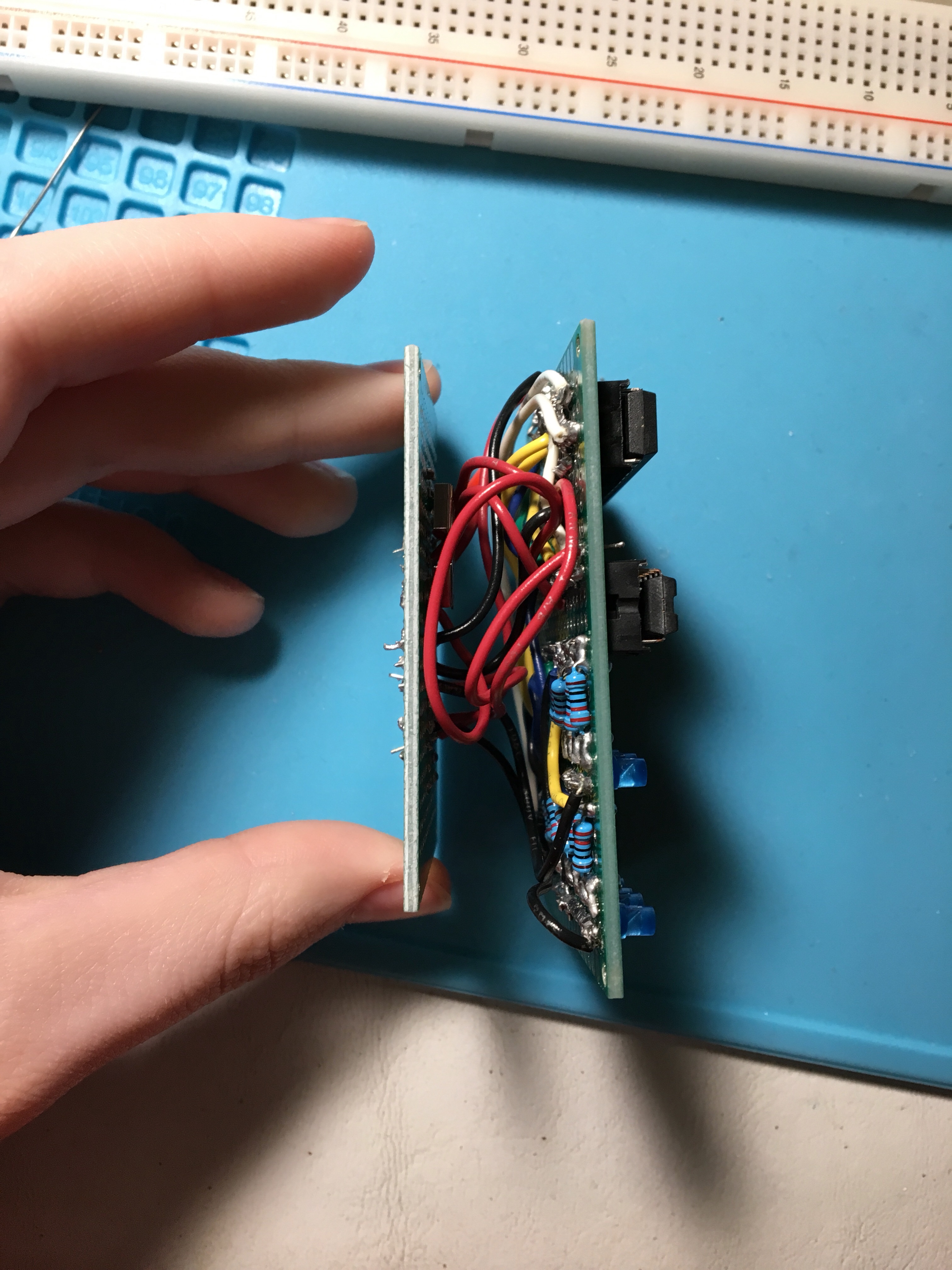
Once everything was Vcc’ed and GNDed, I plugged the microcontroller, shift registers, and battery in….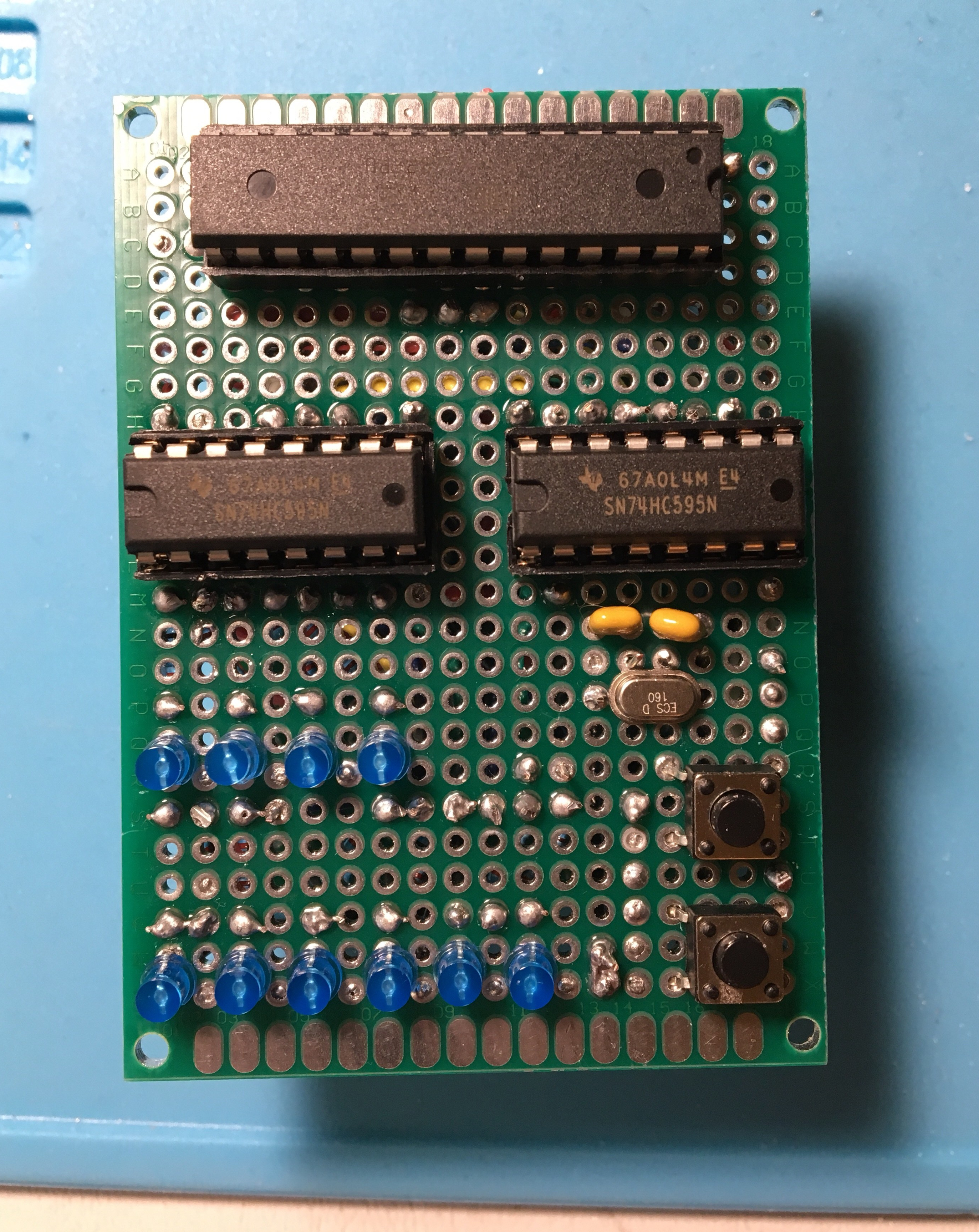
and boom!
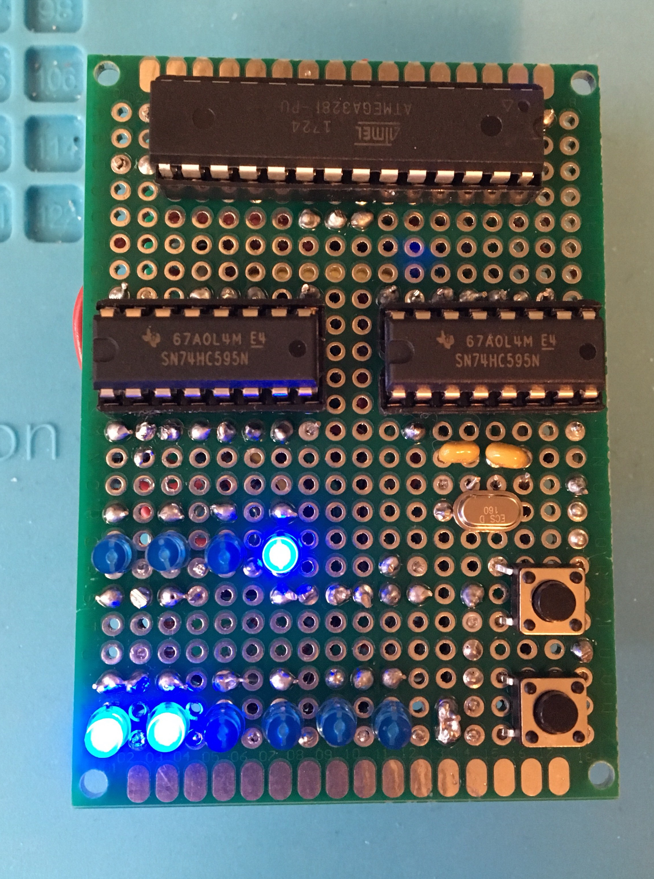
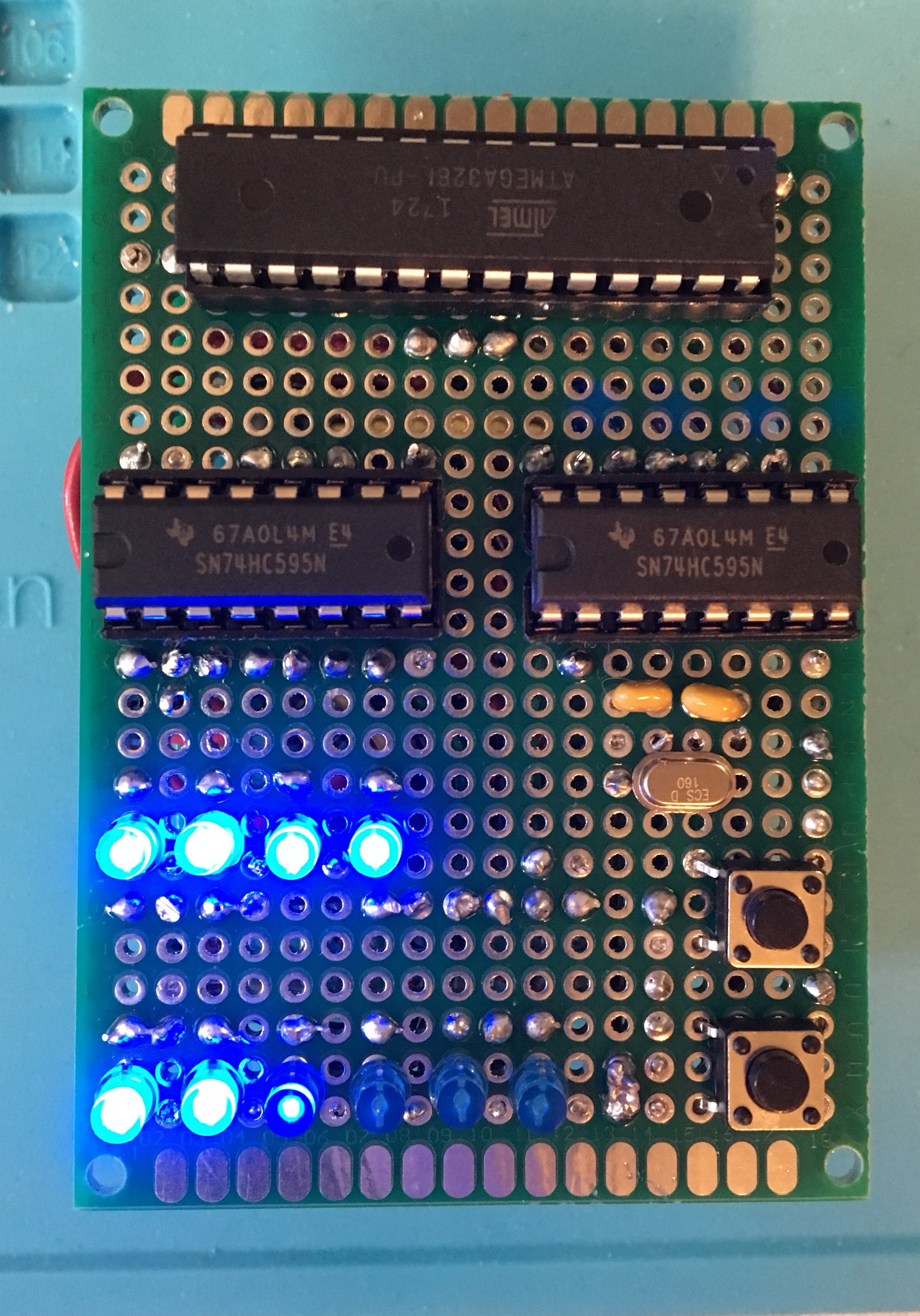
The coin cell battery powered it quite well, and I believe once I start using the deep sleep modules, it’ll be even more efficient. I will have to test how much current the microcontrollers, shift registers, and LEDs are drawing to make sure, of course. The wiring was a little iffy, if I shifted the wires by accident the program would restart. I wasn’t too worried about that, because it worked all at once the first time I plugged it in and didn’t touch it. A little wire debugging wouldn’t hurt in the future, but I’m happy for now.
I’m so proud of how far I’ve come and everything I’ve learned so far. There’s nothing like a project to teach you so many new things and hone your skills. Here’s to more advancements soon!
Again, you can find the ATmega pinouts and my circuit design in this blog post: Prepping the ATmega328P: bootloader burn, fuse-byte programming, and hardware test : binary watch, as well as have access to all my resources on my github repository.
Next steps will require making a new schematic that’s easier to read, start working with the low power modules, and sketch out some experimental PCB design.
{thallia}